SMM News on May 16:
01 What is a wafer
In the wave of modern technology, wafers shine like brilliant stars across various fields of the electronic information industry. The commonly seen solar panels on rooftops cannot do without wafers, a core material.
A wafer is a thin slice composed of silicon, an element located in Group 14 of the periodic table with an atomic number of 14. It is a semiconductor material with unique electrical properties, capable of functioning between conductors and insulators, making it a key material for manufacturing various electronic devices.
02 Classification of wafers
Monocrystalline silicon? Polysilicon? What are their similarities and differences? The fundamental difference between monocrystalline silicon and polysilicon lies in their crystal structures. Silicon atoms are arranged in many crystal nuclei in a diamond lattice. If these crystal nuclei grow into grains with the same crystal plane orientation, monocrystalline silicon is formed. If they grow into grains with different crystal plane orientations, polysilicon is formed.
(I) Monocrystalline silicon wafer
In the field of solar PV, wafers usually refer to monocrystalline silicon wafers. The main function of common monocrystalline silicon wafers is to utilize PV solar energy for power generation and as a raw material for heating. Monocrystalline silicon wafers are cut from high-purity monocrystalline silicon ingots, with a purity requirement typically reaching 5 nines, i.e., 99.999% pure silicon. Monocrystalline silicon has a regular atomic arrangement, presenting a perfect crystal structure. This structure gives monocrystalline silicon wafers excellent electrical and mechanical properties.
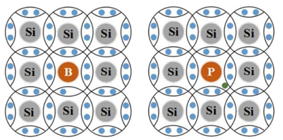
Currently, monocrystalline silicon wafers are mainly divided into two categories: N-type and P-type wafers. The distinction between N-type and P-type wafers primarily lies in the different atoms doped during the intrinsic silicon stage. For example, doping pentavalent elements (such as phosphorus, arsenic) into intrinsic silicon forms N-type monocrystalline silicon, while doping trivalent elements (such as boron, gallium) into intrinsic silicon forms P-type monocrystalline silicon. The following figure shows the lattice structures of N-type and P-type monocrystalline silicon (P on the left, N on the right).
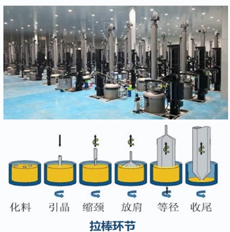
Using high-purity polysilicon as the raw material, crystal pulling technologies such as CZ (Czochralski method) or FZ (float-zone method) are employed to convert polysilicon into monocrystalline silicon ingots. The Czochralski method involves immersing a seed crystal into molten silicon liquid, slowly rotating and pulling it upwards to allow silicon atoms to arrange orderly on the seed crystal, forming a monocrystalline silicon ingot. The float-zone method uses high-frequency induction heating to locally melt the silicon ingot, utilizing the growth characteristics of crystals to obtain high-purity monocrystalline silicon ingots. After obtaining the monocrystalline silicon ingots, they need to be cut into thin slices, followed by processes such as grinding and polishing to obtain monocrystalline silicon wafers with smooth surfaces and precise dimensions.
The main specifications of monocrystalline silicon wafers include: N-type 183, N-type 210, and N-type 210R. These three types of wafers are the mainstream large-sized wafers on the market. The remaining P-type wafers mainly include 182 and P-type 210. Other early mainstream sizes include M6 (166mm), which has been gradually phased out, as well as the transitional size G1 (158.75mm) and the past mainstream size M2 (156.75mm). Additionally, there are rectangular silicon wafers of other models, such as M10D, M10L, M10DL, etc., as well as rectangular silicon wafers measuring 182.2×191.6mm.
(II) Polycrystalline Silicon Wafers
Polycrystalline silicon wafers are cut from polycrystalline silicon ingots. The atomic arrangement of polysilicon is disordered, composed of many small crystallites. Therefore, polycrystalline silicon wafers do not have N-type or P-type distinctions. Due to their disordered arrangement, their electrical performance is inferior to that of monocrystalline silicon wafers, but their preparation is relatively simple and cost-effective. The casting method is commonly used to prepare polycrystalline silicon ingots. High-purity polysilicon is melted and poured into a mold, where it cools and solidifies to form a polycrystalline silicon ingot. The ingot is then cut, ground, and polished to obtain polycrystalline silicon wafers.
Polycrystalline silicon wafers are mainly used in the field of solar cells. Although their photoelectric conversion efficiency is slightly lower than that of monocrystalline silicon wafers, they are still widely used in large-scale PV power generation projects due to their significant cost advantages. Many of the solar panels seen in some solar power plants and household solar power generation systems are made from polycrystalline silicon wafers.
(III) Amorphous Silicon Wafers
Amorphous silicon wafers, or amorphous silicon, are a type of amorphous semiconductor material. Their atomic arrangement lacks obvious periodicity, presenting a disordered state. The common method for preparing amorphous silicon wafers is vapor deposition, such as glow discharge decomposition and sputtering. Glow discharge decomposition involves decomposing gases like silane in a vacuum chamber under the influence of a high-frequency electric field, causing silicon atoms to deposit on a substrate and form an amorphous silicon film. Sputtering involves bombarding a silicon target with high-energy ions, causing silicon atoms to sputter onto a substrate and form an amorphous silicon film.
Amorphous silicon wafers are mainly used in fields such as thin-film solar cells and sensors. In thin-film solar cells, they can be made into flexible solar cells for use in special applications, such as solar backpacks and solar cars. In the sensor field, amorphous silicon wafers can be used to manufacture photosensitive sensors, temperature sensors, etc.
03 Preparation Methods of Silicon Wafers
The manufacturing process of monocrystalline silicon wafers is not complex. The primary raw material is high-purity polysilicon, and the main key steps include crystal pulling, slicing, grinding, detection, and packaging.
(I) Crystal Pulling
Firstly, high-purity polysilicon needs to be transformed into monocrystalline silicon ingots. This process involves two production methods: the Czochralski (CZ) method and the Float Zone (FZ) method. In the field of PV solar energy, the CZ method is commonly used, accounting for 85% of monocrystalline silicon production. The principle involves immersing a seed crystal into molten silicon, slowly rotating and pulling it upwards, allowing silicon atoms to arrange orderly on the seed crystal, forming a monocrystalline silicon ingot.
Firstly, polysilicon and dopants (such as boron and phosphorus) are stacked and placed into a quartz crucible, heated to 1420°C for melting. The molten silicon obtained is a critical step in distinguishing between N-type and P-type materials, as the raw materials added at this stage determine the type. A seed crystal (a small piece of monocrystalline silicon) is slowly lowered to contact the melt. By controlling the pulling speed (approximately 1-5mm/min) and temperature gradient, a monocrystalline silicon ingot is grown. Common diameters include 6 inches (150mm), 8 inches (200mm), and 12 inches (300mm). The figure below shows a demonstration of the crystal pulling process.
(II) Cutting, Grinding, and Polishing
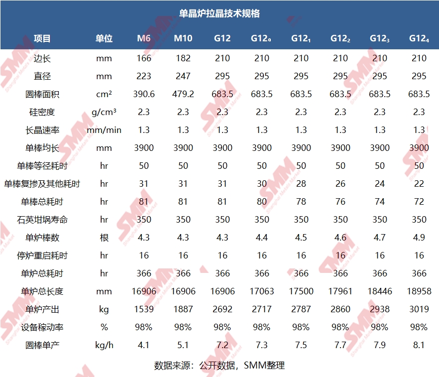
During the crystal pulling process, it is difficult to control the diameter of the monocrystalline silicon ingot. The figure shows the technical specifications for crystal pulling in a monocrystalline furnace.
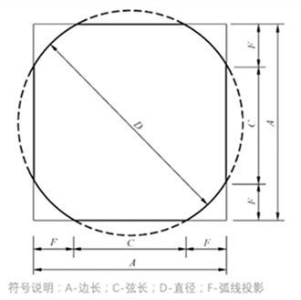
The pulled monocrystalline silicon ingot has its head, tail, and edges removed to obtain a cylindrical silicon ingot. To achieve standard diameters such as 6 inches, 8 inches, and 12 inches, the silicon wafer undergoes outer diameter rolling after crystal pulling, typically requiring the concentricity rate of the silicon ingot to be less than 1%. This is done to eliminate diameter deviations during production. After this, the monocrystalline silicon ingot is squared, transforming the cylindrical silicon wafer into a regular square ingot (e.g., 156mm×156mm, 182mm×182mm, etc.). The squared ingot's surface is polished to remove the oxide layer and burrs, facilitating subsequent cutting. After polishing, the silicon ingot is fixed on a cutting table. The diamond wire is tensioned (the wire spacing depends on the thickness of the silicon wafer). Through the circulation of mortar (cutting fluid + silicon carbide), the diamond wire moves back and forth at high speed (wire speed 10-20m/s), cutting the silicon ingot into thin slices (thickness 150-200μm, with N-type silicon wafers being thinner, reaching below 130μm). The figure below shows a schematic diagram of the side structure of a silicon ingot after crystal pulling.
The thickness of the monocrystalline silicon wafer after the initial cutting is typically 150-200μm (for PV applications). At this stage, the monocrystalline silicon wafer does not meet the requirements for cell manufacturing. The surface of the monocrystalline silicon wafer has certain damage and roughness, necessitating grinding to remove the damaged surface layer and achieve the required thickness and flatness of the silicon wafer. A grinder is used, with silicon carbide abrasive and an alkaline solution (such as NaOH) as the medium, to grind both sides of the silicon wafer, ensuring the surface flatness error is < 5μm. The edges are rounded, and finally, polishing is performed. Special attention should be paid to polishing the edges of the silicon wafer separately to eliminate sharp corners and reduce the risk of edge leakage during cell preparation. The surface of the wafer is made smooth and flat, with a roughness (Ra) ≤ 0.1 nm. At this point, there may still be some other impurities on the surface of the wafer, which require further cleaning.
First, perform alkaline washing: Use a NaOH solution to remove the cutting residue (mortar) and metal ions on the surface. Step-2: Acid washing: Use a HF/HNO₃ mixture to remove the surface oxide layer and heavy metal impurities. Rinsing with deionized water: Multiple ultrasonic cleanings are performed to ensure no particle residues remain on the surface (particle size < 1 μm). After cleaning, the production of the wafer is basically completed. However, the quality of the produced wafer is still unknown. Therefore, final detection is required.
(III) Detection and Packaging
After the wafer production is completed, a series of performance detections are carried out on the wafer to ensure it meets the subsequent cell manufacturing requirements. Each wafer producer has different standards for wafer quality, which are mainly classified into Grade A, Grade B, and Grade C. The quality of the wafer is mainly evaluated in the following aspects: appearance quality, dimensional accuracy, resistivity, minority carrier lifetime, crystal defects, etc. First, measure the physical dimensions of the wafer, including length, width, and thickness. Finally, measure the flatness and related mechanical properties. When measuring electrical properties, the four-point probe method is commonly used to measure the resistivity of the wafer. The resistivity range of N-type wafers is typically 0.5-2 Ω・cm. In addition, minority carrier testing is also required, usually using the microwave photoconductance decay method. Pulse light injects carriers, and a microwave sensor detects the conductivity decay curve to fit and obtain the minority carrier lifetime (τ). It should be noted that this testing method needs to be performed in a darkroom environment. The higher the lifetime, the fewer carrier recombinations, and the higher the cell efficiency. The minority carrier lifetime of N-type wafers is typically 500 μs.
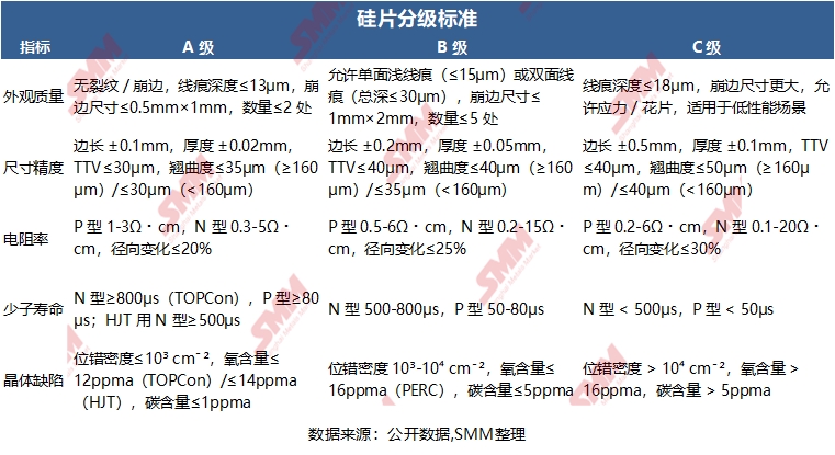
In addition to physical and electrical properties, the impurity content in the wafer is also an important factor in determining the wafer quality, such as oxygen content. Usually, impurities in silicon are classified into two categories: metal impurities and non-metal impurities. To determine metal impurities, ICP-MS (Inductively Coupled Plasma Mass Spectrometry) is commonly used. Typically, a sample of the wafer is taken, acid-dissolved, and then trace metal elements are detected using a mass spectrometer. The total metal impurity concentration is usually required to be ≤ 1×10¹⁵ atoms/cm³. For the determination of carbon and oxygen content, an infrared spectrometer is used: Utilizing the infrared absorption characteristics of silicon-oxygen and silicon-carbon bonds, the oxygen content (Cz wafer oxygen content is typically 1-1.5×10¹⁸ atoms/cm³) and carbon content (≤ 5×10¹⁶ atoms/cm³) are measured.
After a batch of wafers passes the inspection, they still need to undergo packaging before being shipped to the solar cell manufacturing plant. The core objective is to protect the physical integrity and electrical performance stability of the wafer. Through refined packaging design (anti-static, moisture-proof, and shock-proof), the loss of wafers during circulation is reduced. Wafers are typically packaged and transported using wafer packaging boxes.
(IV) Introduction to Auxiliary Materials
Several auxiliary materials are indispensable in the production of monocrystalline silicon wafers. These materials, which can affect the quality of the wafers, mainly include crucibles and diamond wires.
Quartz crucibles are the core consumables for monocrystalline growth in wafer production. The core features of quartz crucibles are high-temperature resistance, high purity, and the absence of black spots and bubbles. The inner wall is usually coated with a high-temperature-resistant film to reduce contamination and erosion of the silicon melt.
Quartz crucibles are typically divided into three layers. The innermost layer is a BaO coating (in direct contact with polysilicon at temperatures above 1420°C), which requires extreme purity (metal impurities <5ppm) and is usually coated with a thickness of 5-10μm. Its purpose is to form a barium silicate protective film to inhibit the erosion of the quartz by the silicon melt. The middle layer mainly provides structural support and is usually made of SiO₂ with a purity of over 99.95%. The outer layer is mainly used to enhance the strength of the crucible and withstand thermal stress.
The second key auxiliary material is the cutting wire, namely the diamond wire used. Diamond wires are classified into two types: resin-bonded diamond wires and electroplated diamond wires. In the field of PV solar energy, resin-bonded diamond wires are typically used for cutting monocrystalline silicon wafers.
Resin-bonded diamond wires consist of two parts: an internal high-carbon steel wire (50-150μm) coated with artificial diamond silicon powder, forming a diamond wire with a diameter of 50-150μm. The carbon steel wire (containing 0.8-1.2% C, with a tensile strength >2500MPa) has its surface fixed with diamond micro powder (particle size 5-40μm, concentration 20-30 particles/mm) through a resin adhesive (phenolic resin + coupling agent). The diamond wire moves at high speed back and forth under the guidance of the guide wheel (wire speed 10-20m/s), while the silicon ingot is vertically cut into the wire mesh at a speed of 0.1-0.5mm/min, completing the process of cutting the silicon ingot into wafers.
04 Development History and Future Trends of Wafers
(I) Wafer Thickness - Thinning
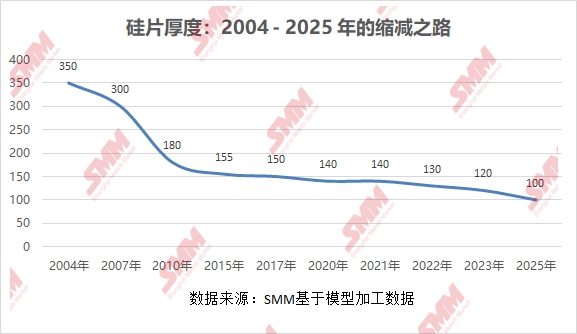
The thickness of wafers has shown a trend of thinning with the advancement of industry technology and the requirement for cost reduction. In the early days of PV enterprises around 2000, wafer thicknesses were mostly in the range of 300μm~400μm, mainly limited by the loss of the slurry cutting technology and the mechanical strength requirements of the wafers. At this time, the loss of polysilicon was relatively high, but thicker wafers were relatively easier to handle.
The period from 2000 to 2010 was a period of rapid breakthroughs in PV technology. During these ten years, the thickness of wafers decreased from 300μm~400μm to 150μm~180μm. The period from 2010 to 2020 was marked by rapid wafer thinning. The primary reason for the reduction in wafer thickness during this phase was the adoption of diamond wire sawing technology, which gradually replaced slurry sawing.
Since 2010, diamond wire sawing technology has continued to advance, with the diameter of the diamond wire continuously decreasing. The improvement in wafer strength has also contributed to wafer thinning. Technologies such as edge passivation and laser doping have enhanced the crack resistance of wafers, supporting the use of thinner wafers. Overall, the development of wafer thickness has evolved from thicker polycrystalline silicon wafers to monocrystalline silicon wafers, transitioning from the initial 300μm~400μm to the current 100μm. Technology has continuously advanced, and wafer thickness has steadily decreased.
(II) Wafer Size - Larger Sizes
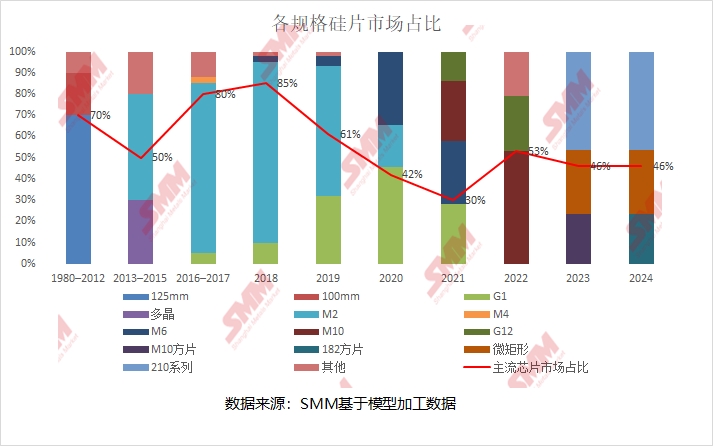
Before 2012, wafer sizes were continuously increasing. In the early stages of wafer production, influenced by semiconductor wafer technology, PV wafer sizes were relatively small and scattered. Moreover, the slurry sawing technology at that time limited both wafer thickness and size, with polycrystalline silicon wafers dominating the market, while monocrystalline silicon wafers were in their infancy.
The period from 2012 to 2018 was marked by the establishment of standardization. During this time, top-tier enterprises jointly introduced the M2 (156.75mm) wafer, which subsequently became the industry's unified standard. It peaked in 2018, capturing 85% of the market share that year. By this time, polysilicon had been gradually replaced by monocrystalline silicon wafers.
Since 2018, the wafer market has entered a phase of competition for larger sizes. In 2018, Jinko introduced the G1 (158.75mm) wafer. In 2019, LONGi launched the M6 (166mm) wafer, which increased the area by 15% compared to the M2, with module power exceeding 400W. In the same year, TCL Zhonghuan introduced the G12 (210mm) wafer, which increased the area by 60.8% compared to the M6, ushering in an era of ultra-high power. In 2020, LONGi, in collaboration with Jinko and JA Solar Technology, jointly introduced the M10 (182mm) wafer, balancing power and industry chain compatibility.
To date, N-type monocrystalline silicon wafers, primarily in sizes of 183mm, 210R, and 210, have dominated the market. As can be seen from the figure, the market has evolved from a variety of wafer sizes in the early stages to a standardized market dominated by a single size in the mid-stage, and now to a market dominated by larger wafer sizes. The three mainstream specifications remaining are 182 square, micro-rectangular, and 210-series.
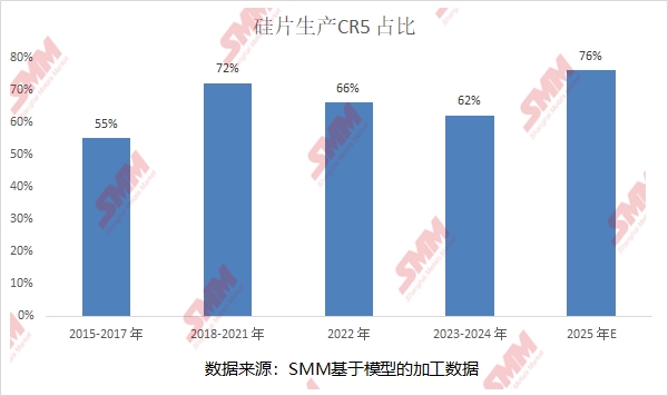
(III) Concentration of Wafer Production Capacity
Since 2015, the overall trend in wafer production capacity has been towards concentration, shifting from a highly competitive market with numerous players in the early stages to a market where the top five enterprises (CR5) account for the majority of the market share. From 2016 to 2020, a duopoly pattern was evident (CR2 exceeding 50%), primarily due to the joint release of the M2-type wafer by these top-tier enterprises, which became the industry's unified standard. Subsequently, after 2021, new entrants (Shuangliang and Gokin Solar) broke the monopoly, causing the CR5 share to pull back to around 60%. In 2024, with the increased production capacity of integrated producers such as Jinko and JA Solar Technology, the CR5 share has further declined. However, the wafer market still demonstrates overall industrial concentration, with a significant decrease in the number of small producers.
05 Wafer Production Trends and Major Producers
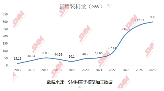
(I) Year-on-Year Growth in PV Installations
In 2015, the National Energy Administration (NEA) clearly defined the "PV Poverty Alleviation" policy for the first time, promoting the implementation of rural distributed PV projects. Since then, China's PV installations have generally shown a year-on-year upward trend. The installations experienced a temporary decline in 2018-2019 due to the 531 Policy and the transition phase from polysilicon to monocrystalline silicon, with policies shifting towards market-oriented competition. In the same year, 2019, the levelized cost of electricity (LCOE) for PV approached that of coal-fired power. Since then, PV installations have entered a phase of rapid year-on-year growth. Nowadays, with the inevitable trend of developing clean energy, installations remain at a high level. Moreover, with advancements in grid connection technology and industrial standardization, distributed PV still holds significant installation potential.
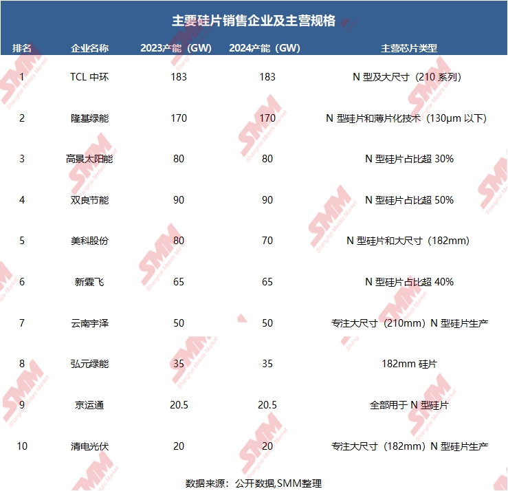
(II) Major Wafer Producers and Their Production Capacities
The following are the major wafer producers. This list primarily includes enterprises that sell wafers externally. Among them, LONGi is an integrated enterprise, but due to its large wafer production capacity, it also engages in wafer exports. However, enterprises such as Jinko and JA Solar Technology, mentioned above, are highly integrated and rarely sell chips externally, primarily using them in-house. Therefore, they are not listed here. The table shows that there are certain differences in the main wafer specifications offered by each producer, but most focus on the production and sale of N-type, large-sized wafers.


![[SMM PV News] Armenia Hits 1.1 GW Solar Capacity,](https://imgqn.smm.cn/usercenter/qQwIB20251217171741.jpg)
![Spot Market and Domestic Inventory Brief Review (February 5, 2026) [SMM Silver Market Weekly Review]](https://imgqn.smm.cn/usercenter/tSwaX20251217171735.jpg)